| Sign In | Join Free | My himfr.com |
|

Shenzhen Hiner Technology Co.,LTD.
Verified Supplier
2 Years
| Sign In | Join Free | My himfr.com |
|
2 Years


| Ask Lasest Price | |
| Brand Name : | Hiner-pack |
| Model Number : | Including 2Inch,3Inch,4Inch,5Inch,6Inch |
| Certification : | ISO 9001 ROHS SGS |
| Price : | 0.85~6USD/PCS(Difference size) |
| Payment Terms : | T/T |
| Supply Ability : | 300~500sets per day |
| Delivery Time : | 15~20 Working days |
Description
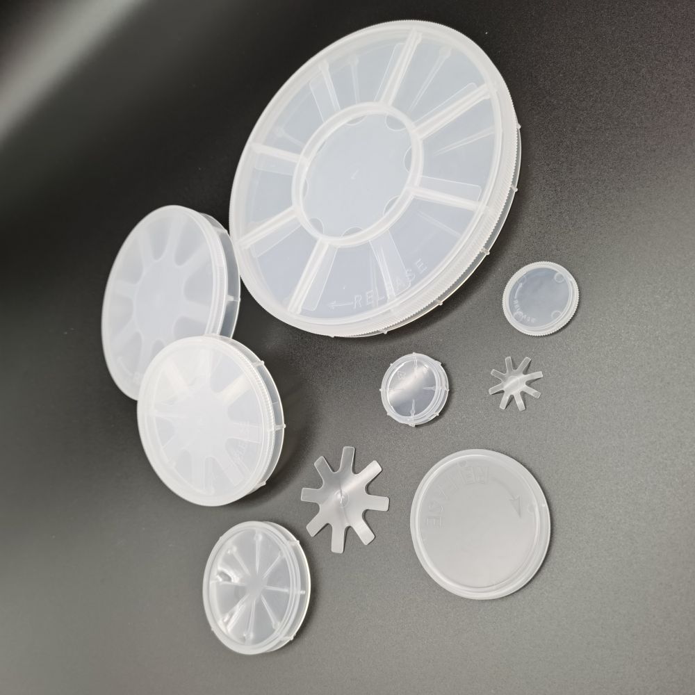
• Each Single Wafer Box includes a spider ring (pressure retention), lid and the base case. The wafer carriers have a conical base to support the wafers at the edges only. The wafers are held in place and secured by a spider spring and locking lid.
| Item Material | PP |
| OEM&ODM | YES |
| Item Color | Transparent |
| Feature | Durable;Reusable;Rcofriendly;Biodegradable |
| Sample | The free samples: choosen from existing products. |
| Packing | Carton or as per customer's request |
| Delivery time | Usually 8-10 working days,depends on order quantity |
R&D laboratory
• Material testing: In research laboratories, wafer boxes are used to store test
samples to ensure their safety and stability during the
experimental process.
• Sample management: facilitates the recording and management of samples of different
materials, improving experimental efficiency.
Photoelectron
• Optoelectronic chips: Crystal round boxes in the field of optoelectronics are used to
protect optoelectronic chips, ensuring their performance and
reliability.

FAQ
Q1:How can I get a quotation?
A1: Please provide the details of your requirements as clear as
possible. So we can send you the offer at the first time.
For purchasing or further discussion, it is better to contact us
with Skype / Email / Phone / Whatsapp, in case of any delays.
Q2: How long will it take to get a response?
A2: We will reply to you within 24 hours of working day.
Q3: What kind of service we provide?
A3: We can design IC Tray drawings in advance based on your clear
description of the IC or component.Provide one-stop service from
design to packaging and shipping.
Q4: What is your terms of delivery?
A4: We accept EXW,FOB,CIF,DDU,DDP etc. You can choose the one which
is the most convenient or cost effective for you.
Q5: How to guarantee quality?
A5: Our samples through strict testing, the finished products
comply with the international JEDEC standards, to ensure 100%
qualified rate.
|
|


